In the fast-evolving landscape of electronics, the demand for advanced circuit board technology has never been higher. Multi-Layer High Density Interconnect (HDI) PCBs have emerged as a leading solution, offering a wealth of advantages that cater to modern electronic requirements.

One of the primary benefits of Multi-Layer HDI PCBs is their ability to enhance performance through increased component density. This is achieved by utilizing microvias and blind/buried vias, allowing designers to create intricate circuit paths while minimizing the overall footprint.
As electronic devices become smaller and more powerful, size reduction is critical. Multi-Layer HDI PCBs accomplish this by supporting more layers in a compact design, ensuring that manufacturers can meet consumer demands without compromising on functionality.
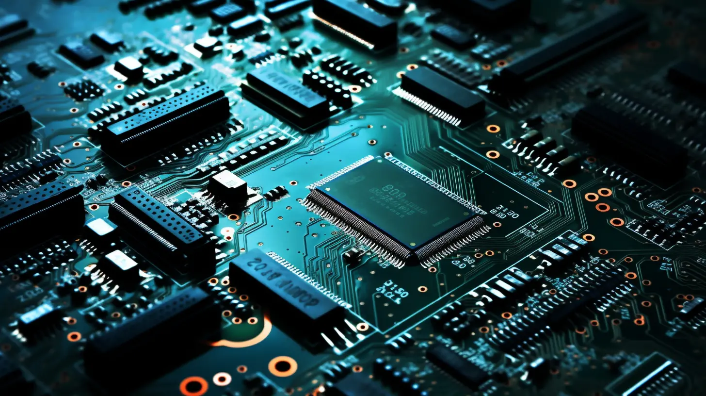
With the integration of advanced materials and fabrication techniques, Multi-Layer HDI PCBs demonstrate improved reliability in various applications. The enhanced thermal management and electrical performance result in a longer lifespan for devices, a critical factor in maintaining competitiveness in the market.
As technology continues to advance, Multi-Layer HDI PCBs are expected to play a pivotal role in the future of circuit board design. Manufacturers who adopt this technology now will be well-positioned to lead in innovation and meet the continuous demands of the electronics industry.
In conclusion, Multi-Layer HDI PCBs represent a significant advancement in circuit board technology. By leveraging their capabilities, companies can enhance performance, reduce size, and ensure reliability, ultimately unlocking innovation in the electronics sector.


 40
|
40
|
 Multilayer PCB circuit board
High conductivity PCB
FR-4 circuit board
Thick Copper PCB
Electronic hardware circuit
Multilayer PCB circuit board
High conductivity PCB
FR-4 circuit board
Thick Copper PCB
Electronic hardware circuit
 192
|
High temperature resistant PCB
HDI PCB Materials
High performance circuit boards
Electronic product reliability
58
|
High durability connector
Hard gold edge connector
market segmentation
472
|
High impedance control
Medical PCB
Laboratory Automation
467
|
Flexible FPC board
Electronic equipment
High frequency applications
Advantages
Circuit Design
192
|
High temperature resistant PCB
HDI PCB Materials
High performance circuit boards
Electronic product reliability
58
|
High durability connector
Hard gold edge connector
market segmentation
472
|
High impedance control
Medical PCB
Laboratory Automation
467
|
Flexible FPC board
Electronic equipment
High frequency applications
Advantages
Circuit Design