
In the rapidly evolving world of electronics, multi-layer PCBs are becoming the backbone of advanced circuit design. But what exactly are they? Simply put, these intricate boards allow multiple layers of circuitry to be stacked, enhancing performance without taking up additional space. And let’s face it, who doesn’t want a more efficient design without sacrificing real estate?
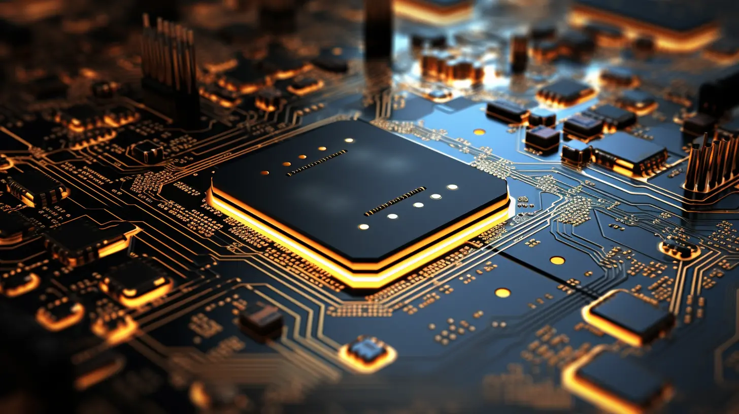
Let’s dive into some perks of using multi-layer PCBs. First off, they provide enhanced electrical performance. By minimizing the distance between layers, these boards reduce signal loss and interference. Secondly, their compact nature means more space for additional components - yes, more gadgets!
Multi-layer PCBs are not just for the fancy gadgets. They find applications in a plethora of devices from smartphones to medical equipment. The reliability they bring to critical systems is unmatched. Imagine a world where your device never fails – that’s the magic of these boards!
In conclusion, multi-layer PCBs are paving the way for the future of electronics. As technology advances, so does the necessity for reliable and efficient circuit designs. Embracing this trend will undoubtedly keep your products competitive and your customers happy! Are you ready to make the switch?

 89
|
89
|
 Precision IC Substrates
High-Speed PCB
Circuit Board Manufacturing
Multi-Layer PCB
Precision IC Substrates
High-Speed PCB
Circuit Board Manufacturing
Multi-Layer PCB
 384
|
HDI PCB
High Density Interconnect Circuit Board
HDI PCB Advantages
Disadvantages of HDI PCB
Electronics Manufacturing
150
|
Hybrid structure PCB
Four-layer rigid-flex PCB
High power applications
203
|
Military PCB
Aerospace PCB
Electronic circuit board solutions
High-performance PCB
68
|
HDI PCB
Medical Devices
High Density Interconnect Circuit Board
384
|
HDI PCB
High Density Interconnect Circuit Board
HDI PCB Advantages
Disadvantages of HDI PCB
Electronics Manufacturing
150
|
Hybrid structure PCB
Four-layer rigid-flex PCB
High power applications
203
|
Military PCB
Aerospace PCB
Electronic circuit board solutions
High-performance PCB
68
|
HDI PCB
Medical Devices
High Density Interconnect Circuit Board


