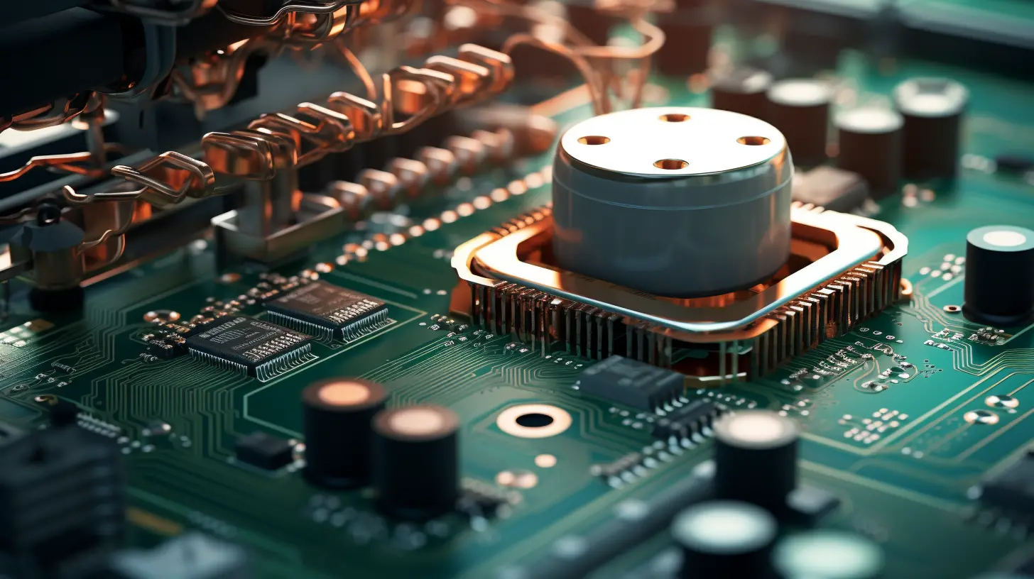
In increasingly complex smart devices, multi-layer PCBs (printed circuit boards) have become an important tool for improving performance. By increasing the number of layers, designers can more effectively manage signal transmission and reduce signal interference, thereby improving the overall performance of the device. 
Multi-layer PCB design not only improves signal integrity, but also effectively improves thermal management. This is because multi-layer circuit boards are better able to disperse heat and reduce the impact of overheating on device performance. Putting these two together is a perfect combination in the world of technology! Imagine playing games on your smartphone while keeping it cool at the same time. It's perfect!
Space is another major design challenge. The use of multi-layer PCBs allows product designers to implement more functions within a limited space, resulting in a more compact design. This is not only aesthetically pleasing, but also greatly improves functionality!
In summary, the flexibility and performance advantages of multi-layer PCBs provide strong support for the technological innovation of smart devices. This not only helps to improve product competitiveness, but also opens up new possibilities for future electronic product design. Most importantly, it is a symbol of modern technological progress - let us welcome the future together!
What do you think about multi-layer PCBs? We welcome you to share your insights and experiences in the comments section!
