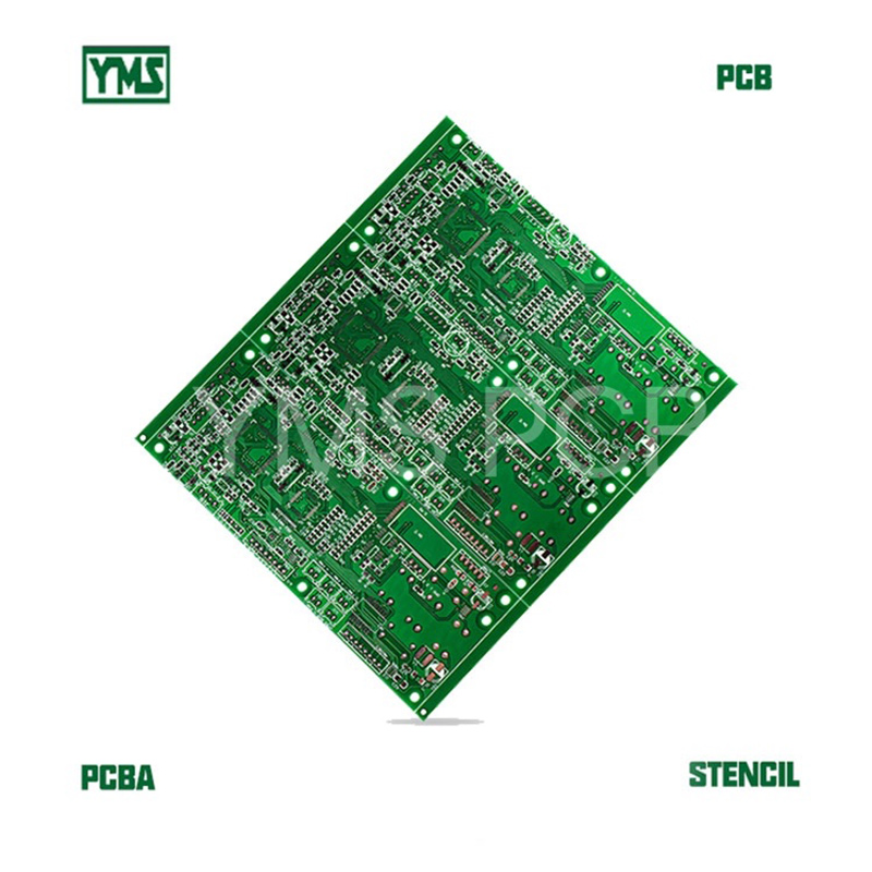
In the ever-evolving world of electronics, the quest for superior performance and reliability never ends. Back drilling technology has emerged as a game-changer, especially in the realm of high-precision multilayer PCBs. But what exactly is back drilling, you may ask? Well, let’s dive into this captivating subject!
This innovative technology is designed to enhance signal integrity by removing excess copper from vias after the board has been manufactured. Imagine cleaning up your circuits for better performance - that’s precisely the magic back drilling works!
Not only does this technique minimize unwanted capacitance, but it also *dramatically improves* communication efficiency. Think of it as giving your electronic devices a much-needed tune-up, ensuring they run faster and cooler.

At the heart of this advanced manufacturing technique is the use of laser processes. These lasers provide the precision required to execute back drilling perfectly, ensuring that manufacturers can keep pushing the boundaries of performance!
In conclusion, integrating back drilling technology into high-precision PCBs not only boosts performance but also transforms the way electronic devices operate. So, next time you hear about a high-tech gadget zipping around at lightning speed, remember: behind that dazzling performance lies the magic of back drilling!
