https://shmuker.oss-cn-hangzhou.aliyuncs.com/data/oss/65aa3975b5fb0b089674052b/65af233dc2e9735675ca9aab/logo.png

Successful case study of eight-layer PCB with hard gold edge connector
2024/10/08
Mingzhenghong Electronics Co., Ltd.
Social interaction
Explore our latest success story, showcasing the use of hard gold edge connectors in eight-layer PCBs, and in-depth analysis of its design advantages and performance improvements.

Successful case study of eight-layer PCB with hard gold edge connector

In the world of connector technology, the charm of hard gold edge connectors is everywhere! Today, we can't wait to share with you the latest success story, showing the excellent application of hard gold edge connectors in eight-layer PCB.
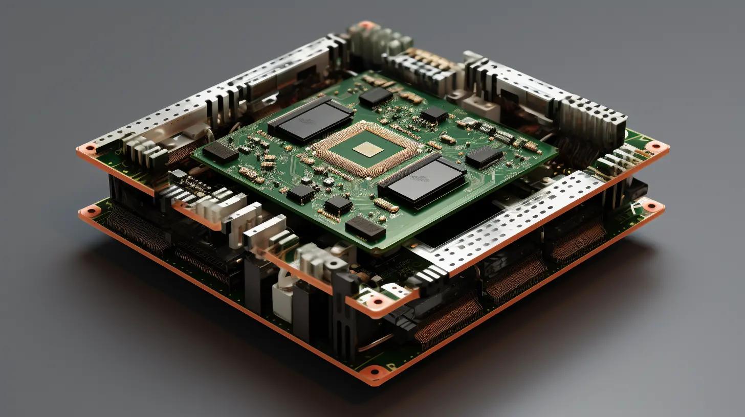
Hard gold edge connector application examples

In this case study, we analyzed how the design advantages of the hard gold-rimmed connector can significantly improve the performance of the eight-layer PCB. It is a perfect combination of technology and aesthetics! Speaking of this, do you also want to know the specific implementation process?

Don’t worry, the following content will give you a deeper understanding of how to create efficient connection solutions! Let’s explore the charm and innovation brought by this advanced technology.
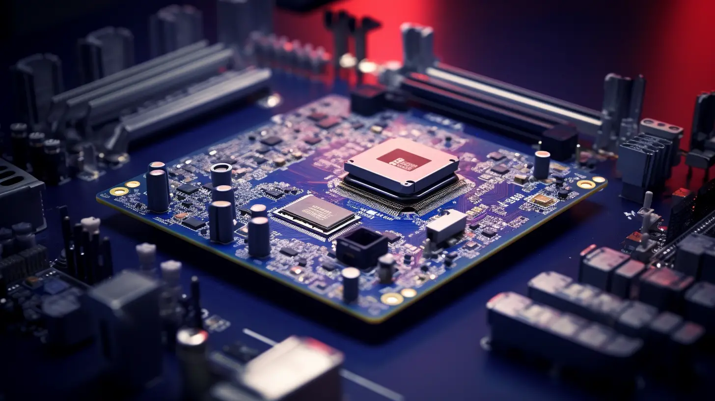
Design in Success Stories

Whether you are an industry expert or a novice, you can benefit a lot from it. Please tell us what you think of this technology in the comment area, or share your project experience. We look forward to your interaction!

Finally, thank you for your attention. We will continue to share more professional knowledge about PCB design to make every connection more stable and reliable!
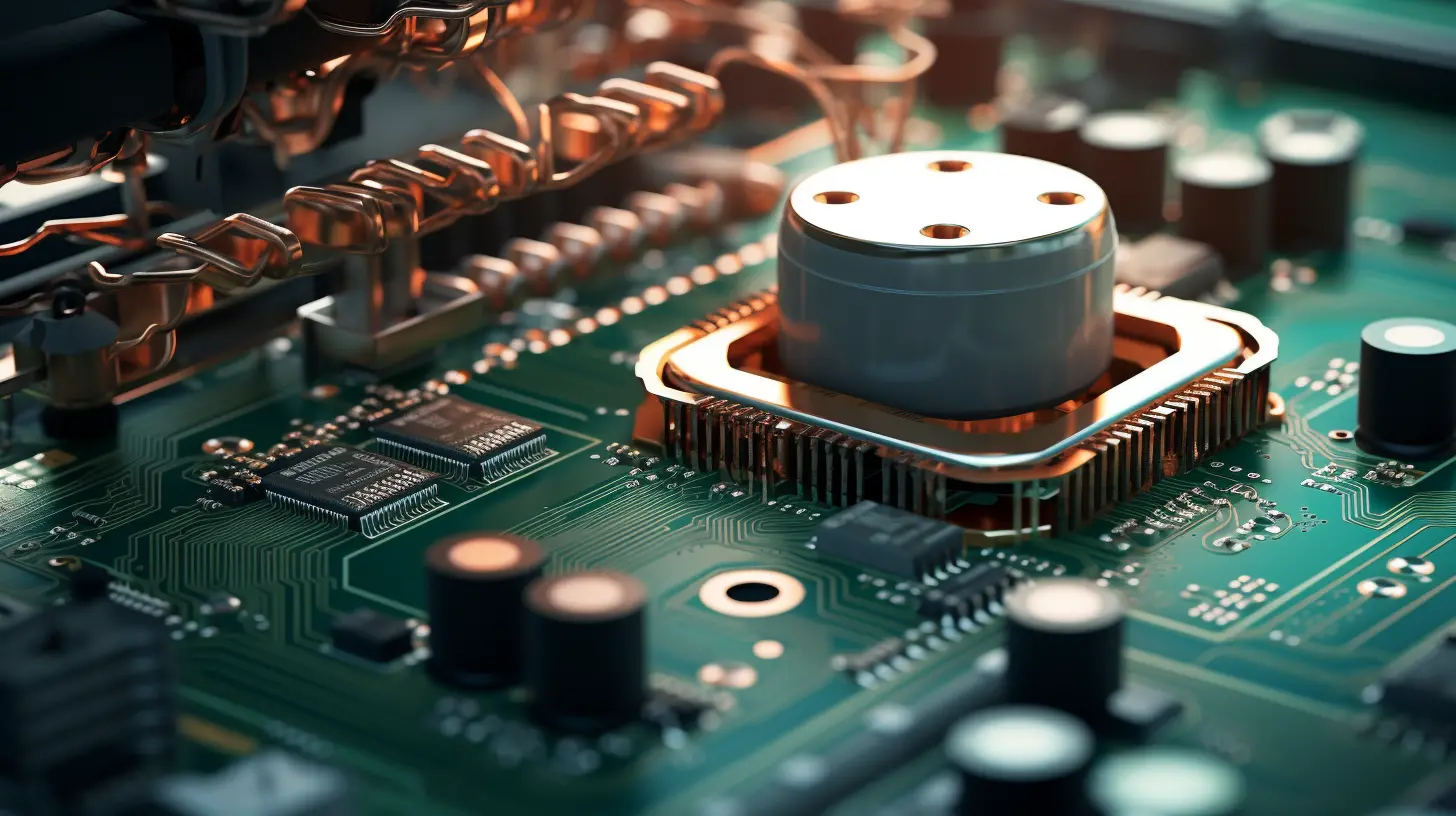
Key points of PCB design
Recommended Products
Related Reading
https://shmuker.oss-cn-hangzhou.aliyuncs.com/data/oss/65aa3975b5fb0b089674052b/65af233dc2e9735675ca9aab/企业照片-4.jpg
2024-09-28
https://shmuker.oss-cn-hangzhou.aliyuncs.com/tmp/temporary/60ec5bd7f8d5a86c84ef79f2/60ec5bdcf8d5a86c84ef7a9a/20240305161110/eye.png 403 | https://shmuker.oss-cn-hangzhou.aliyuncs.com/tmp/temporary/60ec5bd7f8d5a86c84ef79f2/60ec5bdcf8d5a86c84ef7a9a/20240305160636/lable.png Hard gold plating PCB Technology electronic product
https://shmuker.oss-cn-hangzhou.aliyuncs.com/data/oss/65aa3975b5fb0b089674052b/65af233dc2e9735675ca9aab/20240821171142/营销图片-12.jpg
2024-09-28
https://shmuker.oss-cn-hangzhou.aliyuncs.com/tmp/temporary/60ec5bd7f8d5a86c84ef79f2/60ec5bdcf8d5a86c84ef7a9a/20240305161110/eye.png 319 | https://shmuker.oss-cn-hangzhou.aliyuncs.com/tmp/temporary/60ec5bd7f8d5a86c84ef79f2/60ec5bdcf8d5a86c84ef7a9a/20240305160636/lable.png ENEPIG surface treatment High performance PCB board Environmentally friendly process
https://shmuker.oss-cn-hangzhou.aliyuncs.com/data/oss/65aa3975b5fb0b089674052b/65af233dc2e9735675ca9aab/20240821173722/文章配图-4.jpg
2024-09-28
https://shmuker.oss-cn-hangzhou.aliyuncs.com/tmp/temporary/60ec5bd7f8d5a86c84ef79f2/60ec5bdcf8d5a86c84ef7a9a/20240305161110/eye.png 291 | https://shmuker.oss-cn-hangzhou.aliyuncs.com/tmp/temporary/60ec5bd7f8d5a86c84ef79f2/60ec5bdcf8d5a86c84ef7a9a/20240305160636/lable.png High-precision PCB Application Scenario Technical advantages
https://shmuker.oss-cn-hangzhou.aliyuncs.com/data/oss/65aa3975b5fb0b089674052b/65af233dc2e9735675ca9aab/20240821171142/营销图片-14.jpg
2024-09-28
https://shmuker.oss-cn-hangzhou.aliyuncs.com/tmp/temporary/60ec5bd7f8d5a86c84ef79f2/60ec5bdcf8d5a86c84ef7a9a/20240305161110/eye.png 98 | https://shmuker.oss-cn-hangzhou.aliyuncs.com/tmp/temporary/60ec5bd7f8d5a86c84ef79f2/60ec5bdcf8d5a86c84ef7a9a/20240305160636/lable.png Multilayer PCB Electronic equipment Technological breakthrough
Popular articles
Recommended Reading
https://shmuker.oss-cn-hangzhou.aliyuncs.com/tmp/temporary/60ec5bd7f8d5a86c84ef79f2/60ec5bdcf8d5a86c84ef7a9a/thumb-prev.png
TOP
Contact Us