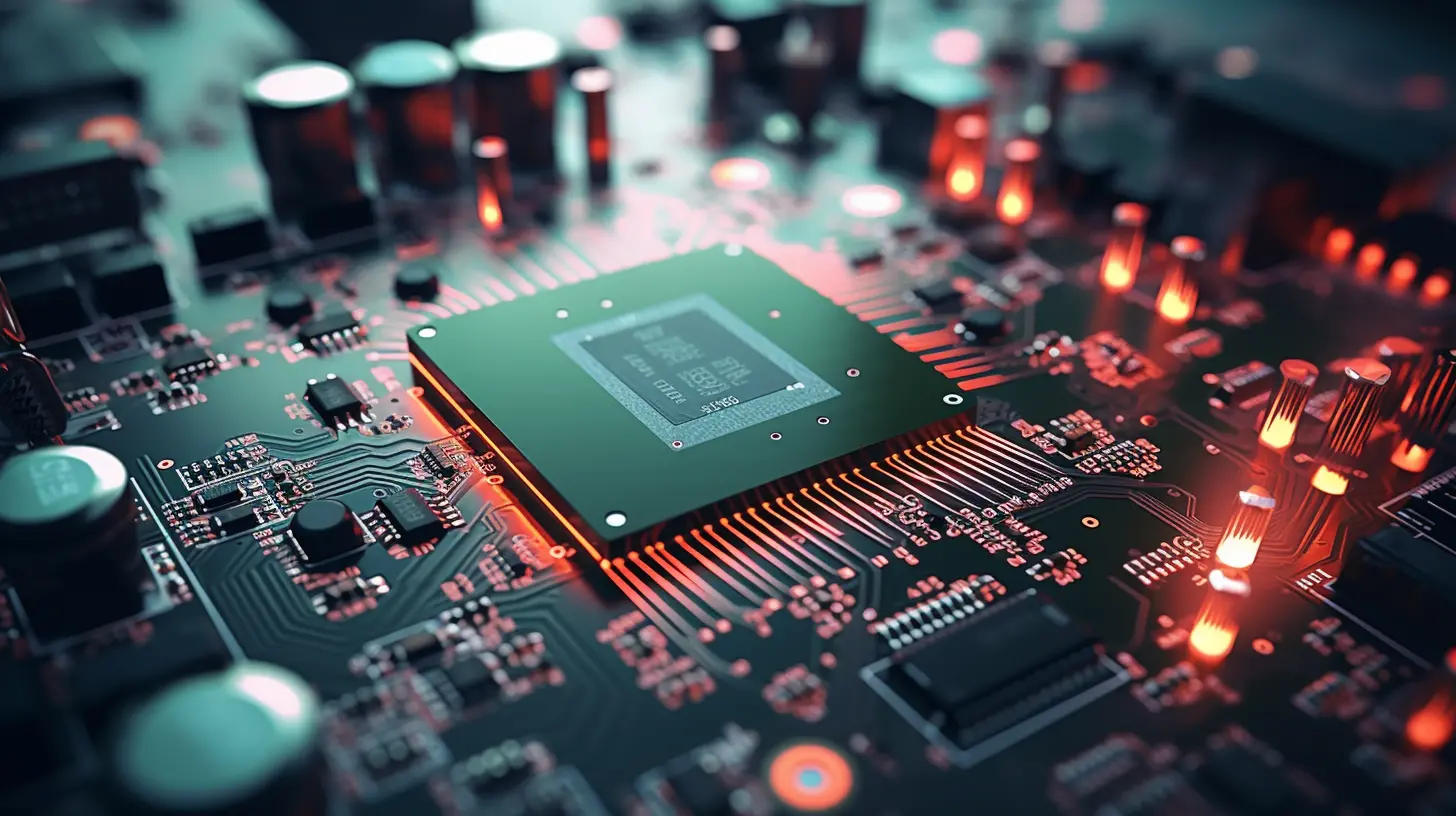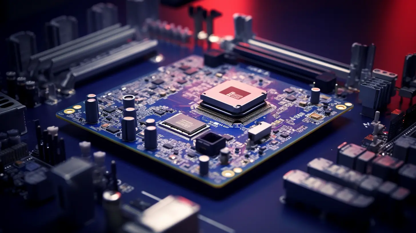
In the context of the rapid development of modern electronic technology, HDI (High Density Interconnect) PCB boards have attracted widespread attention due to their superior performance and miniaturized design. This article will introduce the latest production process of HDI PCB boards to help you explore this exciting field.
Material is one of the key factors that determine PCB performance. High-quality materials not only improve the reliability of circuit boards, but also effectively reduce the failure rate during the production process.  Choosing the right medium, such as materials with low transmission loss, will help improve signal quality and stability.
The multi-layer design of HDI PCB makes the circuit more compact. This not only enhances the functionality of the board, but also provides designers with more design freedom. The connection between layers is superior, and the use of laser micromachining technology can achieve higher-precision circuit processing, improving overall performance.
Laser micromachining technology enables manufacturers to achieve more detailed circuit designs. Let's relax and imagine the application of fine artwork engraved with lasers in the electronic world! This not only improves the accuracy of the product, but also greatly reduces the production cost.
Modern surface mount technology will greatly improve production efficiency. Through optimized material layout and automated equipment, manufacturers can complete mass production more quickly while ensuring the quality of each PCB board. 
Through the optimization of production processes and the application of new technologies, the production process of HDI PCB boards is undergoing a revolution. I hope this article can bring inspiration to your exploration in the field of electronics. Let us work together to promote innovation and development of the industry! 
