The evolution of electronics demands a high level of performance and adaptability, which has led to significant advancements in the design of High-Density Interconnection (HDI) Printed Circuit Boards (PCBs). In this article, we will address the challenges faced in the traditional PCB designs and present innovative flexible design solutions that enhance the functionality of HDI PCBs.
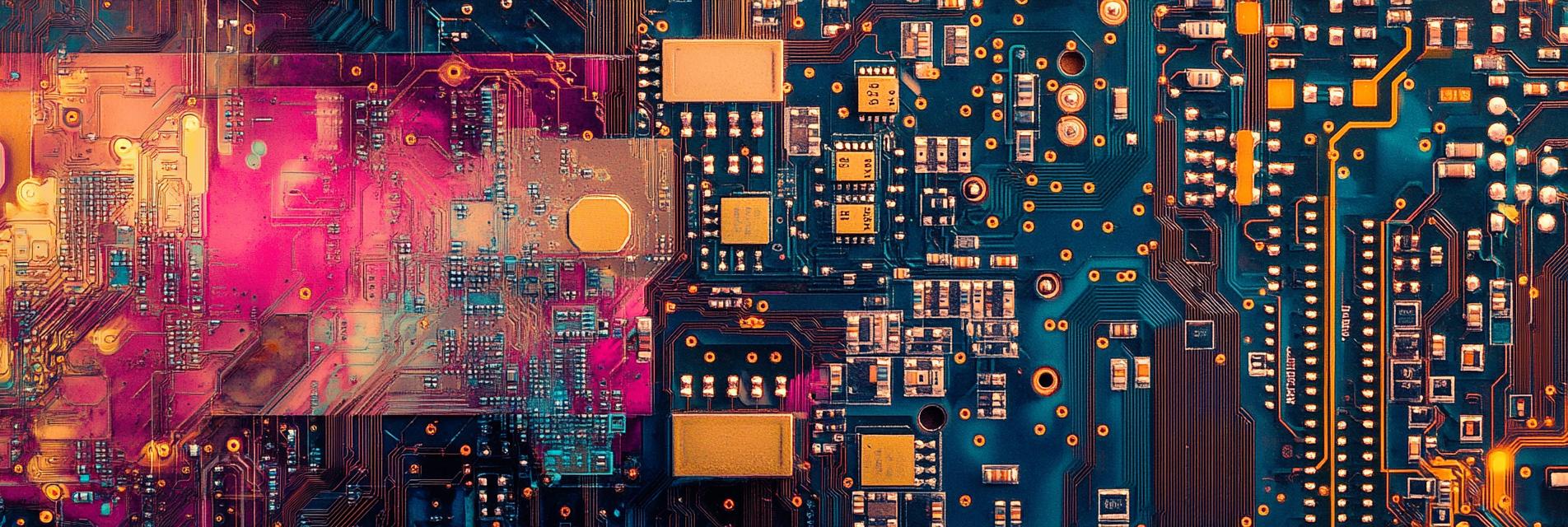
Traditional PCB designs often face limitations that can hinder performance, such as space constraints, heat dissipation issues, and insufficient layer counts for complex circuitry. These challenges can lead to increased costs and longer time-to-market for products. The need for smaller, lighter, and more efficient designs has become more pronounced in the era of portable and wearable electronics.
Flexible design in HDI PCBs introduces several innovative solutions that address the above challenges. By utilizing advanced materials and manufacturing techniques, designers can create PCBs that are not only compact but also capable of withstanding mechanical stress.
1. Enhanced Flexibility: The use of flexible substrates allows for bending and conforming to different shapes, making it suitable for a wide range of applications.
2. Improved Density: HDI technology enables higher interconnection density, facilitating the integration of more components into a smaller area without compromising performance.
3. Thermal Management: Innovations in thermal dissipation technologies ensure that HDI PCBs operate efficiently even in high-temperature environments.
In conclusion, the adoption of innovative flexible design in HDI PCBs addresses the evolving demands of modern electronics while enhancing performance and adaptability. As technology continues to advance, flexible HDI PCBs will play a vital role in enabling cutting-edge applications across various industries.


 475
|
475
|
 PCB products
printed circuit boards
electronic components
PCB manufacturing
custom PCBs
PCB products
printed circuit boards
electronic components
PCB manufacturing
custom PCBs
 319
|
Framed PCBA
PCBA technology
electronic manufacturing
PCB assembly
advanced PCBA solutions
319
|
Framed PCBA
PCBA technology
electronic manufacturing
PCB assembly
advanced PCBA solutions
 457
|
High-speed FPC
Wearable Technology
Electronic Component
489
|
LED Display
PCBA components
Efficient heat dissipation
Aluminum-based materials
Immersion Gold Process
424
|
Hard gold edge connector
Eight-layer PCB
success case
PCB Design
Connector Technology
457
|
High-speed FPC
Wearable Technology
Electronic Component
489
|
LED Display
PCBA components
Efficient heat dissipation
Aluminum-based materials
Immersion Gold Process
424
|
Hard gold edge connector
Eight-layer PCB
success case
PCB Design
Connector Technology


