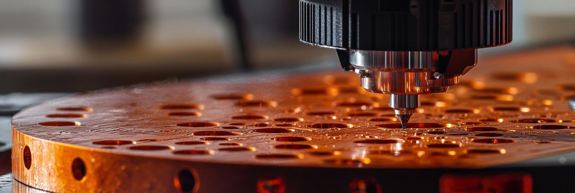
In the rapidly evolving field of electronics manufacturing, the integrity and performance of printed circuit boards (PCBs) are paramount. Laser blind hole technology has emerged as a groundbreaking solution for producing PCBs that can withstand the rigors of high voltage environments. These specialized boards enhance reliability, improve thermal management, and provide unmatched design flexibility, making them ideal for critical applications.
The design of laser blind hole PCBs incorporates features that significantly boost reliability in high-pressure settings. Unlike traditional methods, laser processing minimizes the risk of micro-cracks and other defects during the drilling process. This leads to fewer failures under operational stress, making these PCBs a trusted choice for mission-critical applications.
One of the pressing challenges in high voltage environments is effective heat dissipation. Laser blind hole technology allows for the integration of advanced thermal management features directly into the PCB design. This capability ensures that heat generated during operation is efficiently dissipated, preventing overheating and maintaining optimal performance levels.
Another key advantage of laser blind hole PCBs is the unparalleled design flexibility they offer. Manufacturers can create complex, multilayer designs that are not feasible with traditional PCB construction methods. This flexibility enables engineers to optimize circuit layouts for performance while adhering to stringent space constraints common in high voltage applications.
As the electronics industry continues to innovate, the demands on PCB technology have similarly evolved. Devices used in high voltage environments—such as electric vehicles, renewable energy systems, and advanced industrial machinery—require components that can withstand extreme conditions while ensuring a high level of performance. Laser blind hole PCBs are poised to meet these demands, aligning with the industry's shift towards more compact, efficient, and reliable electronic systems.
The implementation of laser blind hole technology in PCB manufacturing marks a significant advancement in the industry, particularly for applications involving high voltage. With enhanced reliability, improved thermal management, and exceptional design flexibility, these PCBs are set to redefine performance standards in critical electronics applications. As manufacturers seek to balance innovation with reliability, laser blind hole PCBs are emerging as a preferred choice, ensuring that high pressure needs are met effectively.


 363
|
363
|
 Flexible PCB
5G
Communication Devices
Flexible PCB
5G
Communication Devices
 456
|
Precision Engineering Circuit Boards
Semiconductor Test PCB
High Precision PCBs
Flexible Circuit Boards
Multilayer PCBs
456
|
Precision Engineering Circuit Boards
Semiconductor Test PCB
High Precision PCBs
Flexible Circuit Boards
Multilayer PCBs
 85
|
Aerospace grade circuit boards
High Precision PCB
ROGERS 4350B
FR-4 TG150
Electronic performance
Aerospace circuit boards
85
|
Aerospace grade circuit boards
High Precision PCB
ROGERS 4350B
FR-4 TG150
Electronic performance
Aerospace circuit boards
 224
|
5G Smart Terminal
PCB Layout
Market analysis
224
|
5G Smart Terminal
PCB Layout
Market analysis
 231
|
Precision circuit boards
Semiconductor test PCB
High-precision PCB
Flexible printed circuit board
Global Electronic Components
231
|
Precision circuit boards
Semiconductor test PCB
High-precision PCB
Flexible printed circuit board
Global Electronic Components


