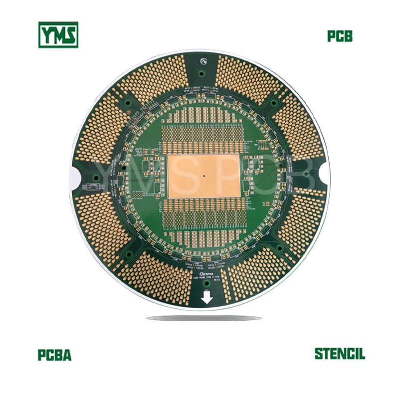
In the world of advanced electronics, ensuring high performance and reliability is paramount. Our High Precision 34-Layer Laser Blind Hole PCB is engineered specifically for the demanding requirements of semiconductor testing applications. This article delves into the features, advantages, and applications of our cutting-edge PCB technology.
At the core of our PCB design is the use of laser blind hole technology and back-drill technology. These advanced techniques enable precise electrical connections while minimizing signal loss, making them ideal for applications where signal integrity is critical. The incorporation of FR-4 TG180 ITEQ material with a thickness of up to 5.0mm ensures that even the most complex circuit designs are supported.
This high-precision PCB boasts several remarkable characteristics:
Quality assurance is paramount in PCB manufacturing. Every board undergoes stringent quality controls to meet IPC standards, ensuring they are ready for the most demanding operational environments. This rigour guarantees that our products maintain functionality and reliability, notably in high-performance electronic testing conditions.
Our High Precision 34-Layer Laser Blind Hole PCB is perfectly suited for:
The High Precision 34-Layer Laser Blind Hole PCB presents an unparalleled solution for industries requiring top-notch reliability and performance. By integrating advanced manufacturing techniques with stringent quality controls, we offer products that meet the highest standards of excellence. Explore the potential of our multilayer PCBs and experience the future of electronic solutions.

 470
|
470
|
 multi-layer PCB
smart factory
advanced manufacturing
electronic components
manufacturing technology
multi-layer PCB
smart factory
advanced manufacturing
electronic components
manufacturing technology
 272
|
Multi-Layer FR-4 PCB
Printed Circuit Boards
Electronics Manufacturing
272
|
Multi-Layer FR-4 PCB
Printed Circuit Boards
Electronics Manufacturing

 336
|
FR-4 TG150 PCB
High performance circuit boards
PCB Technology
161
|
IC Substrate
Impedance control
NO
336
|
FR-4 TG150 PCB
High performance circuit boards
PCB Technology
161
|
IC Substrate
Impedance control
NO


