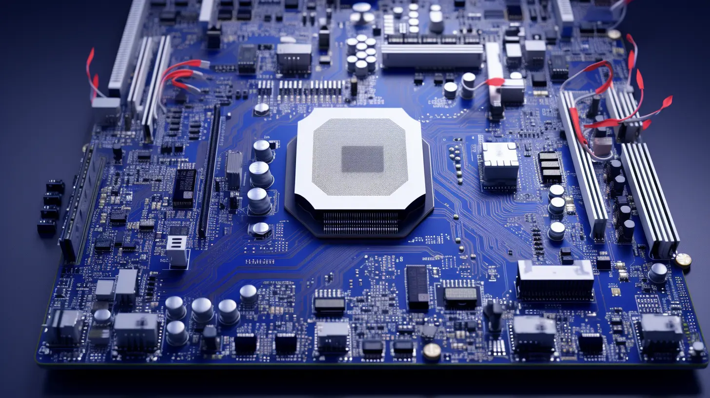
Under the wave of 5G upgrade, high-frequency communication technology has become an important factor in promoting this change. Among them, high-transparency multi-layer PCB has become a key component of 5G base stations and communication products with its unique advantages. It not only improves the signal transmission efficiency, but also meets the strict requirements of high-speed data transmission.
Multilayer PCBs have excellent electrical performance and mechanical stability, especially in 5G applications with frequencies reaching GHz. The high transmittance minimizes signal attenuation and makes data transmission more stable and rapid. Imagine if there were no speed limits on highways, vehicles could travel more efficiently.
As the "hub" of network data, 5G base stations require reliable PCB support. Here, high-transmittance multi-layer PCBs are like the "nervous system" of base station operation, carrying the heavy responsibility of high-speed transmission. Compared with traditional PCBs, their application can effectively reduce energy loss, extend the service life of equipment, and save a lot of costs for enterprises.
Looking ahead, with the continuous advancement of 5G technology, high-transparency multi-layer PCBs will play an increasingly important role. In this context, industry professionals, have you ever encountered challenges in 5G base station applications? Welcome to leave a message below to discuss and share your insights and experiences!
In general, high-transparency multi-layer PCB is a powerful tool for communication technology in the 5G era, and it will bring more innovation and development to the industry. Let us look forward to the arrival of this wireless era!

