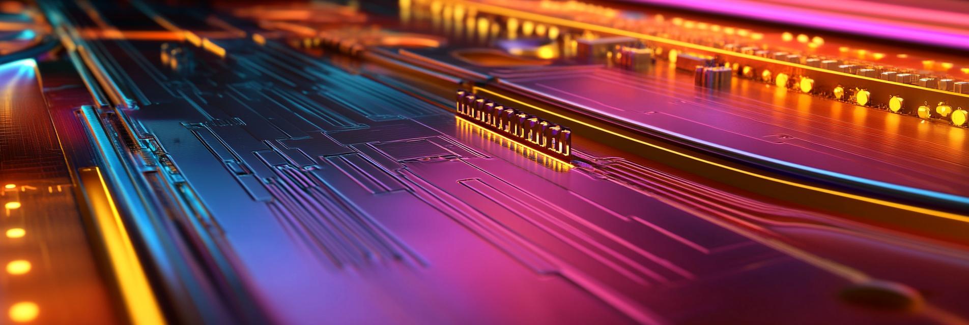
In today's fast-paced technological landscape, the demand for high-performance electronic devices is at an all-time high. As products evolve, so too does the need for advanced technologies that can deliver improved performance without compromising on size or efficiency. One such breakthrough is High-Density Interconnect (HDI) PCB technology. This article delves into the potential of HDI PCBs to elevate product performance in advanced electronic applications.
As electronic devices become more complex, manufacturers face significant challenges in product performance. Traditional PCB designs often lead to issues like signal loss, interference, and overall larger form factors, which hinder the advancement of compact and efficient electronics. In response, the industry has sought innovative solutions to address these hurdles.
HDI PCB technology provides a comprehensive solution to the limitations of traditional PCB designs. By utilizing finer traces and pad sizes, as well as advanced manufacturing techniques, HDIs allow for a greater number of components to be placed in a smaller area. This densification leads to:
The ability to create smaller, more compact designs is one of the most significant benefits of HDI technology. Smaller PCBs not only save space within devices but also enable new form factors and innovative design possibilities, catering to the growing consumer desire for miniaturized electronics.
HDI PCBs utilize blind and buried vias, which enhance signal integrity by minimizing the lengths of electrical paths. This reduction in path length significantly reduces crosstalk and signal loss, ensuring that devices operate at optimal frequencies without interference.
Furthermore, HDI technology allows for the integration of various functionalities into a single board, supporting complex assembly and reducing assembly costs. With the ability to implement multiple layers, it paves the way for multi-functional boards that can support various applications without the need for additional space.
In conclusion, HDI PCB technology stands out as a pivotal advancement in the quest to enhance product performance in advanced electronic applications. By enabling compact designs, improving signal integrity, and increasing functionality, HDI PCBs are set to become integral components in the next generation of electronic devices.

 247
|
247
|
 Automotive PCB
PCB Manufacturing Standards
Automotive Electronics
Automotive PCB
PCB Manufacturing Standards
Automotive Electronics
 75
|
高TG PCB
Edge copper plating
Multilayer PCB
PCB Application
electronic product
80
|
High-performance PCB
Circuit board manufacturing
Innovative Technology
412
|
HDI PCB
Electronic product performance
High Density Interconnect
424
|
High frequency PCB board
5G base station PCB
ROGERS Materials
75
|
高TG PCB
Edge copper plating
Multilayer PCB
PCB Application
electronic product
80
|
High-performance PCB
Circuit board manufacturing
Innovative Technology
412
|
HDI PCB
Electronic product performance
High Density Interconnect
424
|
High frequency PCB board
5G base station PCB
ROGERS Materials


