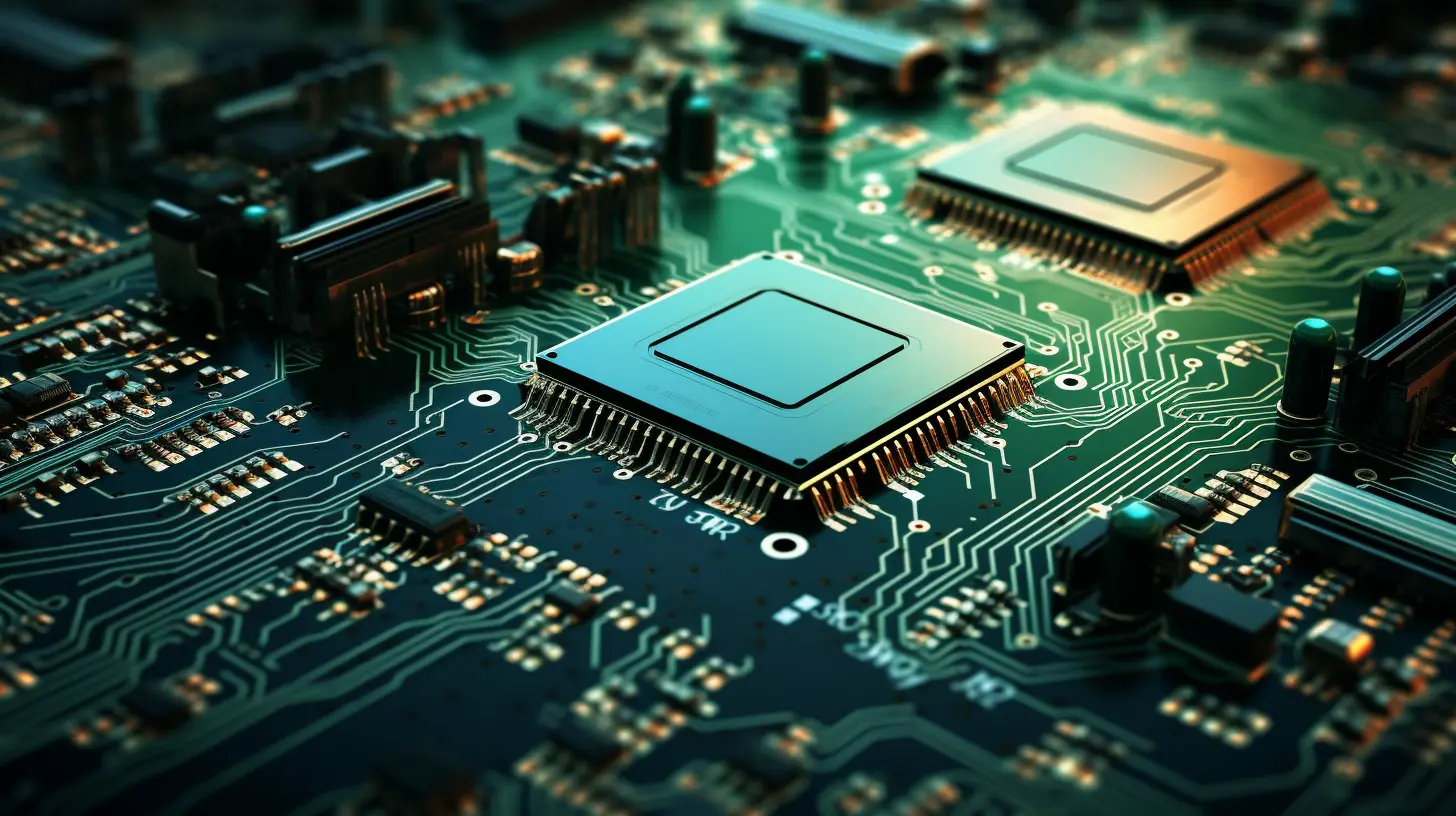
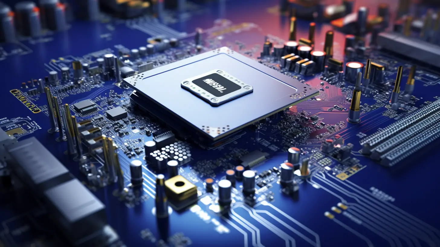
In modern electronic products, high-density interconnect (HDI) PCB boards are like invisible superheroes, quietly improving the performance and reliability of equipment. Faced with increasingly stringent product demands, HDI PCBs, with their high integration and miniaturization characteristics, continue to break through the boundaries of traditional circuit boards and give new life to smart devices.
HDI PCB board, with its fine wire design, can accommodate more components without increasing the space occupied. Imagine that there is an amazing electronic circus in your smartphone, where each component jumps in a small space to ensure the smooth operation of the device!

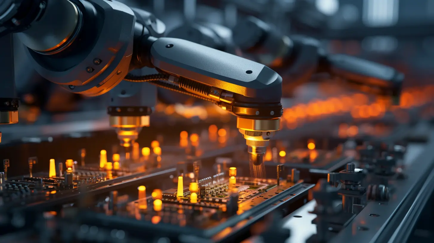
Although HDI PCB technology continues to develop, challenges in design and manufacturing still exist. Designers need to find a balance between miniaturization and complexity, and each circuit is an intellectual competition. However, challenges inevitably bring innovation, and a number of new design concepts and solutions are emerging in the industry.
As smart devices develop towards smaller and more efficient directions, the application of HDI PCB will become more extensive. From smart homes to medical devices, they are effectively driving the intelligence of our lives.

Do you want to know more details about the application of HDI PCB in smart devices? Please leave a message in the comment area and share your views with us! Let us explore the infinite possibilities of future technology together!

