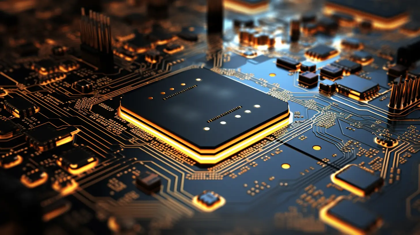
The latest HDI PCB board technology trend analysis is leading the transformation of the electronics industry. High-density interconnect (HDI) technology has been widely used in high-end electronic products such as smartphones and tablets due to its smaller size, lighter weight and excellent electrical performance.
With the development of 5G technology and the Internet of Things, the demand for high-performance HDI PCB boards continues to rise. At present, a variety of new materials and new processes have emerged in the market, such as laser micro-hole technology and multi-layer lamination technology, which further improve the integration and reliability of PCBs.
These new technologies are like "super powers", making electronic products not only compact and lightweight, but also more efficient. In addition, the green manufacturing trend has also promoted the use of recyclable materials. While pursuing performance, companies are also responding to the call for environmental protection.
In-depth analysis of these trends will help companies gain an advantage in the fierce market competition. PCB, which seems ordinary, is a perfect combination of technology and environmental protection. Do you also want to take the lead in this trend?
Through keen insight into market changes, companies will be able to better grasp future development directions.
(P.S. Why not talk to our product team and have a “technology and tradition” exchange of ideas?)

If you are interested in this content, please feel free to leave a message, we look forward to discussing with you.
