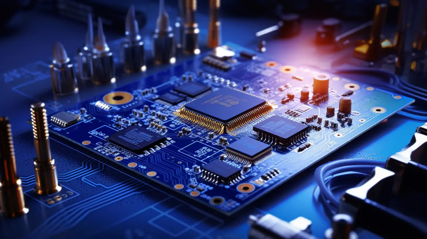
High-frequency multi-layer PCB is a circuit board specially designed to process high-speed signals. They usually have smaller size and higher number of layers to support more circuit functions. In terms of parameter design, higher frequency electrical signals require better materials and designs to reduce signal loss and crosstalk.
In PCB design, choosing the right materials and optimizing the layout are crucial. By applying special design techniques for high-frequency signals, engineers are able to improve signal transmission efficiency and achieve faster data transmission. It's like running a marathon, and a reasonable running strategy can help you win the race.
High-frequency multi-layer PCBs are widely used in many fields such as communications, consumer electronics, medical equipment, etc. For example, in 5G communication products, they play an important role, and nowadays, almost every modern device relies on this technology to some extent.
With the rapid development of smart devices and the Internet of Things, the demand for high-frequency multi-layer PCBs is also rising. It is expected that this field will continue to maintain a high growth trend in the next few years. Enterprises must keep up with this trend in order to stay invincible in the competition.

How much do you know about high-frequency multilayer PCBs? Feel free to share your experience and opinions with us in the comments section! Let's explore this exciting topic together!
